Technology
Creating Imaging Systems
Our strength lies in our full set of core technologies:
(1) Design of analog ASICs;
(2) Development of sensor modules;
(3) Design of optical systems; and
(4) Data analysis technologies for imaging,
which are required for realizing X-ray/gamma ray imaging systems. For this reason, we are capable of in-house development of custom imaging systems from the ground up. In response to clients’ requests, we are also actively involved in designing imaging systems, as well as joint development of elemental technologies such as ASICs and sensors.
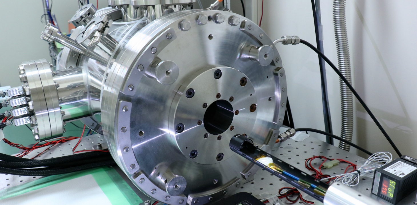
As an example, we would like to describe the flow of development of the Ultra-high spatial resolution Single Photon Emission Computed Tomography (SPECT) device developed in cooperation with Kavli IPMU.
To prevent failures in device development, the first system design (structural design/electrical design) is very important.
To foresee possible risks and to propose to the client a design that avoids risks as much as possible, the accumulation of experience in device development is required.
In addition, to attain the ultimate level of performance, we construct a structural model of the device on a computer, and optimize the device structure by performing accurate scattering/absorption calculations using ray tracing.
Once the system design is complete, we move forward to development of the sensor modules and optical systems, which are system components.
In this process, our core technologies (1), (2), and (3) are utilized.
By integrating these components in the final stages of development, an imaging system is created.
-
System design
System structural design, system electrical design, optimization of device structure via ray tracing, a cost review, and formulation of a development plan. (The above figure is a structural model for ray tracing.) -
Development of components
(Sensor modules, optical systems, etc.)Development utilizing our core technologies
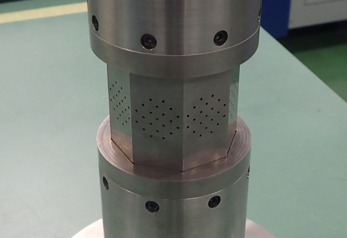
Fine pinhole collimator 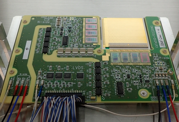
Prototype of the CdTe sensor module -
Integration as an imaging system
-
Calibration and image reconstruction
-
Design technology for analog ASICs
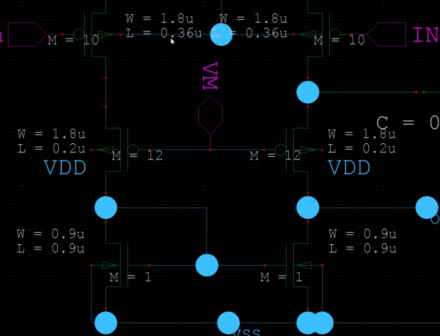
Semiconductor image sensors, such as those composed of silicon (Si) and cadmium telluride (CdTe), comprise an enormous number of pixels. An integrated circuit called an analog ASIC captures the analog signal that occurs on a pixel when a photon enters the sensor, and provides information that serves as the basis for imaging, such as the number of photons and energy detected at each pixel. It is truly a star component for radiation measurement.
Since the analog signals produced by semiconductor image sensors are weak, the design of an analog ASIC requires advanced circuit design technology that amplifies the signal, while simultaneously eliminating noise. Realizing such circuits under various limitations, including system constraints such as power consumption and circuit size, and trade-offs between processing speed and analog performance, provides an opportunity for engineers to display their skills. iMAGINE-X Inc. designs an analog ASIC that meets the demands of our client, based on the proven circuit design IP (Intellectual Property) on radiation measurement that we have accumulated to date. -
Development technologies for sensor modules
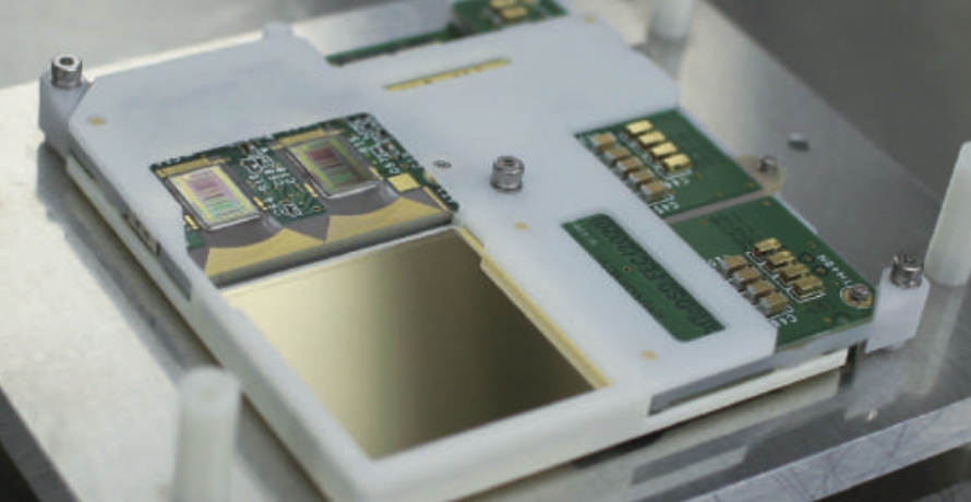
Cadmium telluride (CdTe) sensor module 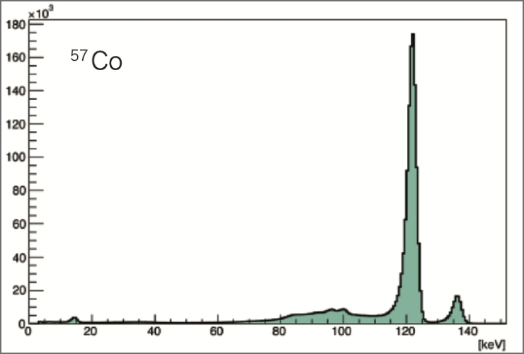
iMAGINE-X Inc. develops unique sensor modules that incorporate a semiconductor image sensor and analog ASIC on an electronic circuit board. Regardless of what powerful image sensors and analog ASICs are available, they are not of value for industrial use unless they can be connected to function with good yield while suppressing increases in noise. In particular, cadmium telluride (CdTe) crystals are fragile and are considered to be very difficult to implement. In recent years, iMAGINE-X Inc. has been working on research and development of image sensors with special electrode structures to improve yield, in cooperation with a CdTe crystal manufacturer.
We have created numerous prototypes to provide a comprehensive evaluation from various perspectives, including an evaluation of spectral performance, bonding strength, and failure mode. As a result, we have discovered promising electrode structures, and have completed our unique large area CdTe sensor module. That module is our CdTe double-sided strip detector (CdTe-DSD). A large effective area (32×32 mm2) is provided, with fewer readout channels and low power consumption. A special analytical algorithm using both anode and cathode signals provides an extremely high energy resolution of 2.5% (FWHM) at 122 keV for the thick (2 mmt) detectors.
This CdTe-DSD is embedded in the mass-production model, “XCam- CdTe” of iMAGINE-X Inc. In addition, it has been highly evaluated, with an offer from NASA (the National Aeronautics and Space Administration) to implement it as a candidate focal plane detector for the next generation of hard X-ray telescopes for astronomical observation. -
Design technologies for optical systems
Optimization of parameters for manufacturing collimators using ray tracing 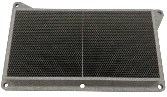
Tungsten collimator made via 3D printer Parts that have the function of changing or limiting the path of light are called optical systems. In humans, the crystalline lens of the eyes plays that role. Since X-rays and gamma rays are not refractive, components called collimators which limit the path of light are used for imaging. However, since there is a trade off between the spatial resolution and efficiency of collimators, it is often difficult to propose designs that fully meet a client’s initial requirements. In such cases, we first thoroughly explain to our clients the trade-offs of optical systems that are peculiar to X-ray/gamma ray imaging, re-organize requirements and conditions such as the size of the subject, the expected number of photons, the minimum required spatial resolution, etc., and decide on the collimator specifications together with our clients.
iMAGINE-X Inc. has developed unique calculation code to determine manufacturing parameters such as the diameter, length, and septal thickness of the collimator. The spatial resolution of the collimator and efficiency requirements serve as the input for the calculation, which determines the manufacturing parameters that maximize performance.
In some cases, for a more refined design, we create a collimator model on a computer, calculate photon scattering and transmittance at the septa using ray tracing, and optimize the manufacturing parameters including these effects. These design technologies have been fully applied to the collimator mounted on the mass-production model, “XCam-CdTe” of iMAGINE-X Inc. Furthermore, based on the latest metal 3D printer technology, we have successfully “printed” collimators optimized for the “XCam-CdTe” that are made of pure tungsten. -
Data analysis technologies for imaging
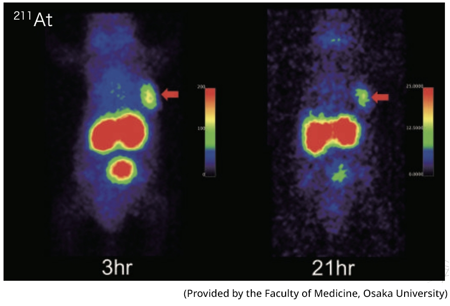
Distribution of At-211 in tumor-bearing mice. The red arrow indicates a tumor. 3D simultaneous visualization of multiple nuclides (Tc-99 m, In-111, I-125). Tc-99m is displayed in red, In-111 in green, and I-125 in cyan. (Takeda et al., IEEE TRPMS, 2023) In imaging systems, if the sensor module is considered to be the eyes, the data analysis technology for imaging can truly be defined as the brain. Data analysis, also referred to as image reconstruction, is the star of medical imaging, and at the same time is one of the most challenging development cases in software.
The reason for this difficulty is that it is necessary to image the distribution of radioisotopes with high quantitative accuracy. To meet this requirement, it is not enough to simply implement an imaging algorithm in software. This is because the devices that are actually assembled display individual characteristics, such as deviations from design values, and therefore, it is necessary to appropriately incorporate information representing such individuality into the data analysis.
The process of acquiring information that represents the individuality of the devices is called calibration, which can bring an imaging system to life. iMAGINE-X Inc. is a start-up company in which experimental physicists have been deeply involved in its founding and operation. As a result, the company has outstanding calibration technology to meet the strict demands of science. This is why the images provided by iMAGINE-X Inc. have high quantitativity.